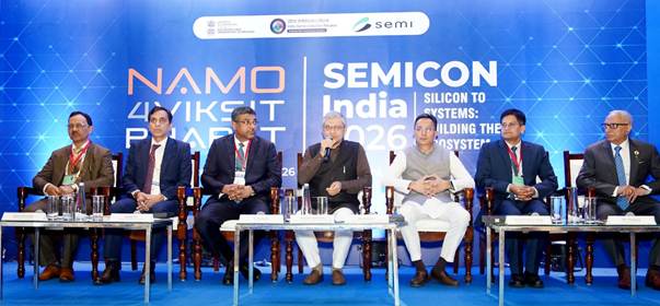
Union Minister for Electronics and Information Technology, Ashwini Vaishnaw, on September 17 outlined the implementation approach and emerging investment momentum under Semicon 2.0, highlighting the Government’s focus on developing the complete semiconductor ecosystem in India.
Addressing the media during SEMICON India 2026, Vaishnaw said that while Semicon 1.0 focused on laying the foundation for India’s semiconductor industry, Semicon 2.0 is aimed at putting the wider ecosystem in place and scaling capabilities across the semiconductor value chain.
The Minister said that investment commitments of around ₹1 lakh crore (approximately USD 11–12 billion) have already been received under the Semicon 2.0 ecosystem. These commitments are expected to translate into significant economic activity and employment, with close to 1 lakh new employment opportunities expected to be created across the semiconductor ecosystem. The investments are expected to materialize over the next two to three years, with companies announcing their respective investments as and when they receive the required board and shareholder approvals.
Six pillars to deepen the semiconductor ecosystem
The Minister outlined the Six broad pillars through which Semicon 2.0 will deepen India’s semiconductor capabilities:
Design ecosystem:
The first pillar focuses on scaling India’s semiconductor design ecosystem by supporting both start-ups and large companies. The approach will include support for scaling fabless companies, access to funding and venture capital, customer discovery and stronger protection of intellectual property.
The Government is targeting 200 semiconductor design start-ups under the expanded approach. The Minister noted that 20 of the 105 semiconductor start-ups supported during the first phase have already secured Venture Capital funding, describing this as a significant achievement and a basis for scaling up the target under Semicon 2.0.
The design ecosystem will also support companies in moving beyond individual chip design towards systems design, enabling Indian talent and companies to address increasingly complex technology requirements.
Machines and materials:
The second pillar will strengthen India’s ecosystem for semiconductor manufacturing equipment, machines and materials.
The Minister highlighted the growing interest of global capital equipment companies in establishing operations in India, including capabilities for design as well as manufacturing. He said that India’s established design capabilities can support global equipment manufacturers in setting up design operations, generating high-quality employment for Indian youth.
Companies establishing manufacturing operations can also benefit from India’s developing precision manufacturing ecosystem, which serves multiple sectors including aerospace, aviation, semiconductors and advanced electronics.
Fabs:
The third pillar focuses on expanding semiconductor fabrication capabilities across different technologies, including display, memory, silicon, compound and logic fabs. The Minister said that confidence among global semiconductor companies is increasing and that interest in establishing semiconductor manufacturing capabilities in India is growing.
Advanced packaging:
The fourth pillar focuses on advanced semiconductor packaging capabilities. With increasing importance of advanced packaging in improving efficiency and system-level performance, the Government will support the development of capabilities in this area as an important part of India’s semiconductor ecosystem.
Research and Development:
The fifth pillar will promote applied R&D involving industry, government and academia. Under this approach, industry will be encouraged to propose R&D projects, with funding participation from industry and Government and involvement of academic institutions. The objective is to develop applied technologies and achieve tangible outcomes that can strengthen India’s semiconductor capabilities.
Talent development:
The sixth pillar focuses on expanding India’s semiconductor talent base. The Minister said that around 400 universities and institutes are already engaged in semiconductor chip-design education under the first phase. Semicon 2.0 will seek to upgrade the curriculum so that students who acquire foundational chip-design capabilities can also progress towards systems design.
In addition, the Government has set a target of training 1 lakh technicians over five years. This will involve partnerships with industry and international institutions, including institutions such as ITRI, Taiwan, to establish training capabilities aligned with the requirements of India’s emerging semiconductor manufacturing facilities.
Focus on building the ecosystem around semiconductor manufacturing
The Minister emphasised that the objective of Semicon 2.0 is not limited to establishing individual semiconductor manufacturing facilities but to build a complete ecosystem around them.
He highlighted the importance of developing domestic capabilities in capital equipment, materials, gases, chemicals, precision manufacturing and supply chains. Such capabilities, he said, would help create a deeper and more resilient semiconductor ecosystem and support India’s long-term growth in the sector.
The Minister also highlighted the growing importance of resilient global supply chains and said that India is seeing increasing interest from semiconductor companies looking to diversify and strengthen their supply chains.
Global competitiveness remains central to semiconductor manufacturing
The Union Minister said that global competitiveness in terms of quality and cost has remained a key consideration from the selection of semiconductor projects through construction and production.
He said that the semiconductor facilities that have entered commercial production are competing in the global market, with production capacity being taken up by customers. He also noted the rapid pace of capacity creation at the facilities currently being established.
11 MoUs and 5 Announcements to strengthen semiconductor value chain
As part of SEMICON India 2026, 11 MoU exchanges and announcements were undertaken covering semiconductor manufacturing, packaging, materials, equipment, design, talent development and related ecosystem capabilities.
Key agreements and announcements included:
Suchi Semicon Pvt Ltd and eInfochips Pvt Ltd exchanged the first batch of commercial devices.
Tata Electronics and Nexperia B.V. entered an MoU covering semiconductor wafer manufacturing, assembly and test, technology collaboration and innovation.
Tata Electronics and Ascendas First Space entered an MoU for developing a 363-acre vendor park to accelerate the semiconductor fab supplier ecosystem in Dholera, Gujarat.
Tata Electronics and Fujifilm Corporation entered an MoU to support localisation of critical semiconductor materials for India’s semiconductor manufacturing ecosystem.
Tata Electronics and JSR Corporation entered an MoU for supply of photoresists and advanced chemicals for Tata Electronics’ fab in Dholera, Gujarat.
Tata Electronics and BESI Singapore Pte. Ltd. entered an MoU focused on building advanced semiconductor packaging capabilities in India.
Tata Electronics and Semiconductor Laboratory (SCL) entered an MoU covering semiconductor design services, process technology, supply-chain localisation and talent development.
Tata Electronics and Gati Shakti Vishwavidyalaya, in collaboration with L&T EduTech and Jacobs Solutions, entered an MoU for talent development in semiconductor facility engineering and infrastructure systems.
Kaynes Semicon and OptoML India entered an MoU to jointly develop advanced semiconductor packaging and System-on-Module solutions.
Kaynes Semicon, GridCrest Technologies and Sensesemi entered an MoU to explore opportunities in packaging, assembly and testing.
India Semiconductor Mission and Intel India launched an ‘Introduction to Semiconductors’ course.
Intel India and New Age Makers’ Institute of Technology (NAMTECH) entered into an MoU for developing a future-ready workforce in AI and semiconductor technologies.
HORIBA inaugurated its HORIBA KOACH Experience Centre.
Sensesemi Technologies Private Limited, Bengaluru and GridCrest Technologies Private Limited, Delhi entered into an MoU for smart metering solutions.
Six ChipIN Regional Centres were announced for expanding access to chip-design capabilities and democratising semiconductor design across the country.
Announcement of commercial production of CDIL semiconductors and association for development of packages with Shindengen Electric Manufacturing Company, Japan.
India’s semiconductor journey moves towards a full-stack ecosystem
According to the Minister, the semiconductor industry is highly complex and requires sustained efforts across multiple layers of the value chain. Semicon 2.0 has therefore been designed to build capabilities not only in chip manufacturing but also in design, equipment, materials, advanced packaging, research, talent and supply chains.
He said that India’s semiconductor journey will require a calibrated and long-term approach, with the objective of establishing an ecosystem capable of supporting sustained growth over the coming decades.
The Government’s approach under Semicon 2.0 is aimed at enabling India to emerge as a trusted and resilient participant across the global semiconductor value chain while creating high-quality employment and strengthening domestic technological capabilities.
SEMICON India 2026 which runs till September 19th at Yashobhoomi , New Delhi, features more than 600 participating companies and is expected to attract around 50,000 visitors, with representatives from 52 countries, more than 400 executives and over 150 speakers. The exhibition features six Country Pavilions representing Japan, South Korea, Malaysia, the Netherlands, Singapore and Sweden, along with 12 State booths, a Startup Pavilion, Innovation Showcase, Student Hackathon and Workforce Development Pavilion.
Source: PIB