
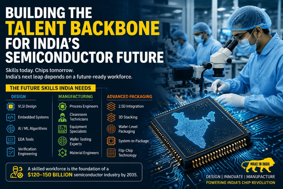
India’s semiconductor ambitions are grand. The country wants to build a semiconductor value chain worth $120-150 billion by 2035, become a global leader in chip design and emerge as one of the world’s top destinations for advanced packaging. But achieving these goals will require more than investments in fabrication plants and policy incentives. It will require people.
According to NITI Aayog’s report Future of India’s Semiconductor Industry, talent could be one of the defining factors in determining whether India succeeds in its semiconductor journey. While the country has established itself as a global hub for semiconductor design, significant skill shortages remain across manufacturing, testing, packaging and hardware research.
The challenge stems from the complexity of semiconductor production itself. “Semiconductor manufacturing involves intricate processes,” the report notes. Technologies such as lithography, etching and deposition require precision at the nanometre level, where even minor deviations can impact chip performance. These processes demand highly specialised engineers, technicians and researchers.
Building the Talent Backbone for India’s Semiconductor Future
2.5D • 3D • SiP • Flip-Chip
Process Engineers • Cleanroom • Testing • Materials
VLSI • AI/ML • Embedded Systems • EDA • Verification
India’s strengths are already visible in chip design. The country hosts a large share of the world’s semiconductor design talent and has become an important base for global chip companies. However, the report highlights that advanced packaging, testing and fabrication continue to face skill shortages. It also points out that while India’s software and design capabilities are strong, hardware R&D infrastructure and expertise are still evolving.
To address these gaps, NITI Aayog has outlined the future skills that will power the semiconductor industry. In design, expertise will be required in VLSI design, embedded systems, AI and machine learning algorithms, analog design, verification engineering and Electronic Design Automation (EDA) tools. These skills are becoming increasingly important as artificial intelligence drives demand for more specialised and power-efficient chips.
Manufacturing presents an even bigger challenge. Future semiconductor facilities will need process engineers skilled in lithography, etching, deposition and ion implantation, along with cleanroom technicians, equipment specialists, wafer testing professionals and material engineers. These roles form the foundation of semiconductor fabrication and quality control.
The fastest-growing opportunity may lie in advanced packaging, an area where India hopes to build global leadership. Skills related to 2.5D integration, 3D stacking, wafer-level packaging, system-in-package technologies and flip-chip packaging will become increasingly valuable as chipmakers look for new ways to improve performance beyond traditional transistor scaling.
The report’s message is clear. Semiconductors are not merely a manufacturing challenge; they are a talent challenge. As India races to become a significant player in the global chip industry, the country’s ability to train engineers, researchers, technicians and packaging specialists at scale could determine whether its semiconductor ambitions become reality. In the coming decade, the most valuable asset in India’s chip ecosystem may not be a fab or a machine, but a skilled workforce capable of building the technologies of the future.