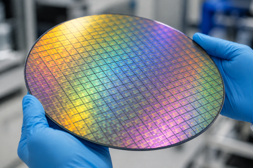
A wafer is a thin, circular slice of semiconductor material—most commonly ultra-pure silicon—used as the foundation on which integrated circuits and other electronic devices are built. It is one of the most important starting materials in semiconductor manufacturing.
Silicon wafers are typically produced from high-purity silicon that is formed into a cylindrical single-crystal ingot. The ingot is then sliced into thin discs and polished to create an extremely flat, clean surface. Semiconductor manufacturers use this surface to build transistors and other circuit structures through processes such as photolithography, deposition, doping and etching.
A single wafer can contain hundreds or even thousands of identical integrated circuits, depending on its size and the complexity of the chips being manufactured. After fabrication, the wafer is cut, or diced, into individual pieces called dies. These dies are subsequently packaged to become usable semiconductor components.
Wafer size matters. Modern semiconductor manufacturing commonly uses 300-mm (12-inch) wafers. Larger wafers allow manufacturers to produce more chips from a single piece of material, potentially improving manufacturing efficiency and reducing cost per chip.
Wafers are not limited to silicon. Semiconductor manufacturing can also use materials such as gallium arsenide (GaAs), gallium nitride (GaN) and silicon carbide (SiC) for specialised applications.
In simple terms, the wafer is the canvas on which a semiconductor chip is built. Its purity, size, flatness and defect levels can directly influence manufacturing yield and chip production economics.