

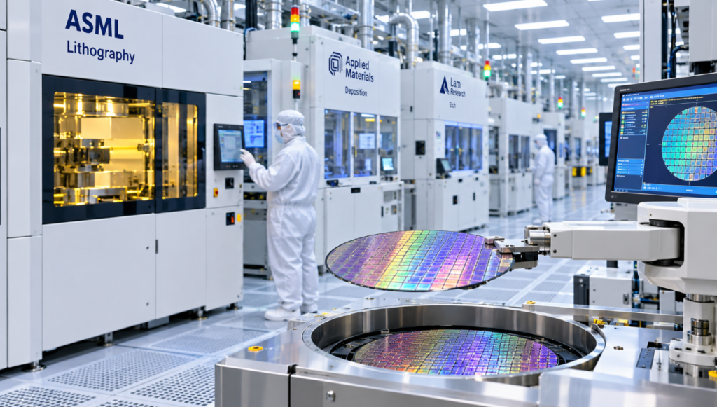
India’s semiconductor ambitions are gathering pace, with billions of dollars being committed to setting up chip manufacturing facilities. But building a semiconductor plant is not just about putting up a factory and installing production lines. It requires some of the most advanced machines in the world, many of which are supplied by a handful of companies based in the US, Europe and Japan.
From printing microscopic circuits on silicon wafers to detecting defects that are invisible to the human eye, each stage of chip manufacturing requires specialised equipment. These machines are critical to determining how efficiently a plant operates and how many usable chips it can produce.
For India, this presents another challenge. While the country is trying to build its semiconductor manufacturing ecosystem, it will continue to depend on global suppliers for much of the machinery and technology required to make chips.
Lithography: Printing circuits on silicon wafers
Every chip starts with a pattern of tiny circuits that must be transferred onto a silicon wafer. This is done using lithography machines, which use light to print intricate designs on a light-sensitive coating called photoresist.
The Netherlands-based ASML is the world’s leading supplier of advanced lithography equipment and the only commercial supplier of extreme ultraviolet (EUV) lithography machines. Japanese companies Nikon and Canon are also important players, particularly in other lithography segments.
Deposition: Building the layers that make a chip
A semiconductor chip is built by adding multiple extremely thin layers of different materials to a silicon wafer. Deposition machines perform this job, laying down insulating and conducting materials that eventually form transistors and electrical connections.
US-based Applied Materials and Lam Research, Japan’s Tokyo Electron and the Netherlands-based ASM International are among the major suppliers. They offer different technologies, including chemical vapour deposition (CVD), physical vapour deposition (PVD) and atomic layer deposition (ALD).
Etching: Removing unwanted material
Once the circuit patterns are transferred onto a wafer, the next step is to remove selected portions of material to create the required structures. This is where etching machines come in. They use chemical processes or plasma to remove unwanted layers without damaging the areas that need to be retained.
Lam Research, Applied Materials and Tokyo Electron are among the leading global suppliers of etching equipment.
Ion implantation: Giving chips their electrical properties
For a chip to function, different parts of the silicon wafer need to have specific electrical properties. Ion implantation machines help achieve this by introducing controlled amounts of electrically active atoms into the silicon. The process, known as doping, is essential for creating transistors and other semiconductor components.
Applied Materials and US-based Axcelis Technologies are among the key suppliers in this segment.
Cleaning and polishing: Keeping wafers free of defects
Chip manufacturing involves several stages, and even tiny particles or chemical residues left behind can affect the final product. Wafers therefore need to be cleaned repeatedly during production. Japan’s SCREEN Holdings, Tokyo Electron and Lam Research are among the companies supplying wafer-cleaning systems.
The wafer surface also needs to remain extremely flat as new layers are added. Chemical Mechanical Planarisation (CMP) machines achieve this by combining chemical and mechanical processes to polish the surface. Applied Materials and Japan’s Ebara are major suppliers.
Inspection and metrology: Finding the smallest defects
A defect that is difficult to see with the naked eye can make an entire chip unusable. Inspection and metrology equipment helps manufacturers examine wafer surfaces, measure microscopic structures and identify defects during production.
US-based KLA is one of the leading suppliers of inspection and process-control systems. Applied Materials and Japan’s Hitachi High-Tech are also important players.
For India, setting up semiconductor fabs is only one part of the larger challenge. The country will also need access to this entire ecosystem of machinery, components, materials and technical expertise.
Over time, developing domestic capabilities in precision engineering, equipment manufacturing and servicing could open up opportunities for Indian companies. Reducing dependence on imported machinery will not happen overnight, but it could become an important part of India’s effort to build a stronger semiconductor manufacturing base.


